 Skip to content
Static Sign-Off
Maximizing design & functional verification efficiency for:
Real Intent static sign-off products lead the market in breadth, precision, performance, and capacity.
FAST
![]()
HCL used this methodology to successfully verify connectivity and glitches on an active SoC design using Real Intent’s SafeConnect in a few days.
This is in contrast to several weeks work required with alternative methods.
– Arun Selvaraju, HCLTech
PRECISE
![]()
STMicroelectronics ran Real Intent Meridian RDC and a competitive tool on a dual CPU subsystem with 150,000 gates, 15 clock domains, ~25,000 CDC paths and ~450,000 RDC paths.
Meridian RDC achieved a 25X reduction in noise, and a ~4X reduction in runtime and RAM usage.
– Julien Faucher, ST Microelectronics
USER EXPERIENCE
![]()
NVIDIA has been a customer of Real Intent since 2000. We are extremely happy with the products, they are a regular part of our flows, and the quality of technical support is excellent.
Real Intent is a reliable business partner for us because of their friendly business practice and dedication to make their customers successful.
– Dan Smith, NVIDIA
![]()
![]()
![]()
![]()
![]()
![]()
![]()
![]()
![]()
![]()
![]()
![]()
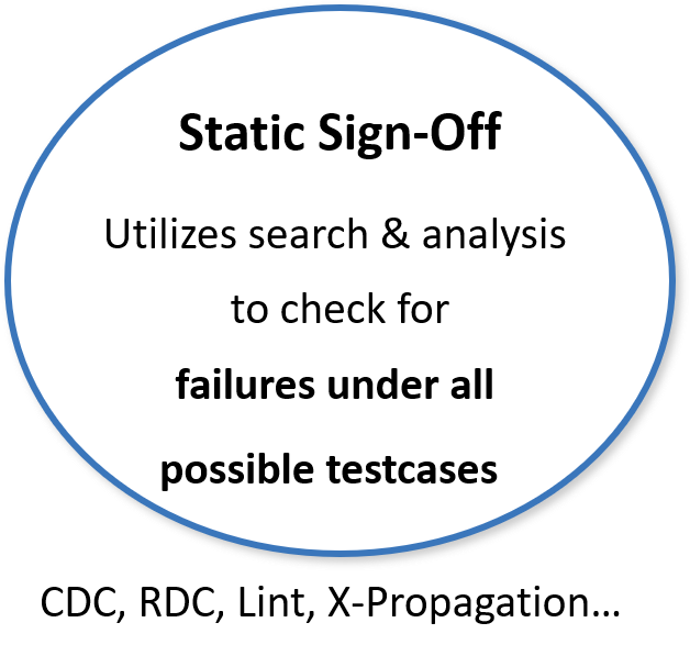
What is Static Sign-off?
Static sign-off uses search and analysis to check for design failures under all possible test cases. Static sign-off technologies can address functional (Clock Domain Crossing, Reset Domain Crossing, Linting, X-Propagation, DFT, Connectivity, Glitch…), layout (DRC), and timing (STA) domains. Real Intent’s focus is functional static sign-off.
Real Intent provides intent-driven static sign-off tools to improve digital design efficiency by accelerating early functional verification .
Its product capabilities for eliminating complex SoC failure modes include: clock domain crossing sign off from RTL through gate level, including multimode CDC; reset domain crossing sign off, advanced RTL linting & analysis, and connectivity & glitch sign-off.
Real Intent products lead the market in breadth, precision, performance, and capacity, with more than 50 major semiconductor and systems company customers.